Surface Finish and Final Processes
Surface Finish and Final Processes
Overview
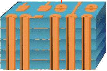
Section titled “Overview”Once the solder mask covers the traces, the copper at the pads remains exposed — unprotected, it would oxidize and undermine soldering. The surface finish (G stage) dresses this copper in an anti-oxidation “protective coat”, while the final processes (H stage) complete profiling, electrical testing, final quality inspection, and packing.
This article concludes the series, ending with a recap of the full 19-step route.
Surface Finish (G Stage)
Section titled “Surface Finish (G Stage)”Every conventional PCB has copper layers; unprotected copper oxidizes and degrades, directly affecting soldering. There are seven common protective finishes:
| Finish | Full name | Key point | Advantages |
|---|---|---|---|
| HASL | Hot Air Solder Leveling | The board is fully coated with solder, then high-pressure hot air blows off the excess on the surface and in the holes and levels the rest; leaded and lead-free versions | Low cost; stays solderable throughout the process |
| OSP | Organic Solderability Preservative | Forms a thin, uniform protective layer on the copper | Cost comparable to HASL; good coplanarity; lead-free process |
| Plating Gold | Electroplated Nickel Gold | Electroplates nickel and a protective gold layer onto copper | Good solderability; flat surface; long shelf life; withstands multiple reflows |
| ENIG | Electroless Nickel Immersion Gold | Chemical displacement deposits a nickel-phosphorus layer, then a gold layer on top | Good solderability; flat surface; long shelf life; withstands multiple reflows |
| Gold Finger | — | Electroplated nickel-gold with a different gold composition (hard gold, wear-resistant) | Wear-resistant, low contact resistance; used for edge connectors |
| Immersion Silver (IS) | — | Immerses a 0.1–0.6 μm silver layer onto the copper | Good solderability; flat surface; a natural HASL replacement |
| Immersion Tin (IT) | — | Immerses a 0.8–1.2 μm tin layer onto the copper | Good solderability; flat surface; relatively low cost |
Selection usually depends on: soldering process (lead-free/leaded), shelf life, cost, and appearance requirements (ENIG has become a common choice for high-end products).
Final Processes (H Stage)
Section titled “Final Processes (H Stage)”01 Profiling
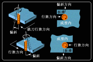
- Purpose: cut the board to the customer-specified dimensions
- Principle: mechanical cutting by CNC machines
- Main material: router bits
- Common forms: CNC routing, and V-cut (V-shaped scoring) — used for panel pre-scoring so finished boards snap apart along the groove; requires controlling the cut depth and remaining web thickness

02 Electrical Test
- Purpose: bare-board testing of PCB electrical performance (opens and shorts) to meet customer requirements
- Trade-offs among test methods:
| Method | Principle | Pros | Cons | Best for |
|---|---|---|---|---|
| Dedicated | Custom bed-of-nails fixture | Fast throughput | Probes cannot be reused; high fixture cost | High volume |
| Universal on Grid | Universal grid fixture | Lower fixture cost | High equipment cost | Medium-high volume |
| Moving Probe (flying probe) | Two probes move in X/Y/Z to test each net’s endpoints in turn | No fixture; low cost | Low throughput | Samples, small batches, rush samples |
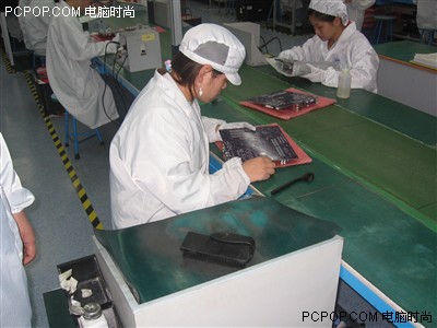
03 Final Inspection and Laboratory
Final inspection/lab is the last quality review in the process, in two categories:
- Inspection items (appearance and dimensions): outline dimension, hole-to-edge distance, board thickness, hole diameter, line width/space, annular ring, and more
- Laboratory items (reliability): solderability, peel strength, micro section, thermal shock, ionic contamination, moisture and insulation resistance, impedance, and more
04 Packing and Shipping
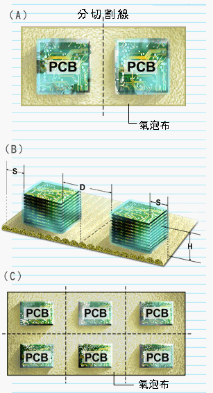
The board is packed as the customer requires and shipped — completing the full journey of a PCB.
The Full 19-Step Recap
Section titled “The Full 19-Step Recap”Expanding the eight stages into one line gives the complete PCB manufacturing route:
1. Inner layer 2. Lamination 3. Exposure 4. Developing 5. Etching6. Strip 7. Lay-up 8. Pressing 9. Drilling 10. PTH11. Lamination 12. Exposure 13. Developing 14. Cu+Sn plate 15. Strip16. Etching 17. Tin strip 18. Silkscreen 19. Surface finish → final processes → shippingNotice: the photoimage transfer and DES logic — “laminate → expose → develop → etch → strip” — appears three times (inner layer, outer layer, solder mask, in different forms). That is the process main thread emphasized in the first article.
Summary (Series Wrap-up)
Section titled “Summary (Series Wrap-up)”- The seven surface finishes each have trade-offs; the ENIG/OSP/HASL choice directly affects solderability and cost
- The final processes handle three things: cut the profile (routing + V-cut), test opens/shorts (three test methods), and inspect before shipping (appearance + reliability checklists)
- Full recap: board cut → inner layer → lamination → drilling → metallization → outer layer → silkscreen → surface finish → final processes — 19 steps across eight stages
You have now walked the complete professional PCB manufacturing process. Recommended next reads:
- Chapter 24 (PCBA Manufacturing and Soldering) — assembling the bare board into a PCBA
Every step from “design file to manufactured part” deserves to be seen with your own eyes (or in a video). Understand the process, and you will make better designs.
We provide ESP32 ODM design-to-manufacturing services. From prototype to production — the team behind this tutorial can build it with you.
Talk to us →