PCB Manufacturing Overview
PCB Manufacturing Overview
Overview
Section titled “Overview”You have designed your circuit in KiCAD, exported the Gerber files, and sent them to a board house — but how exactly does a bare copper-clad laminate turn into a finished PCB? Understanding the professional manufacturing process helps you make better design decisions: why design rules exist and why prototypes and mass production differ.
This chapter breaks down the eight major stages of professional PCB manufacturing. It pairs well with Chapter 24 (PCBA Manufacturing and Soldering). This first article builds the big picture.
What Is a PCB
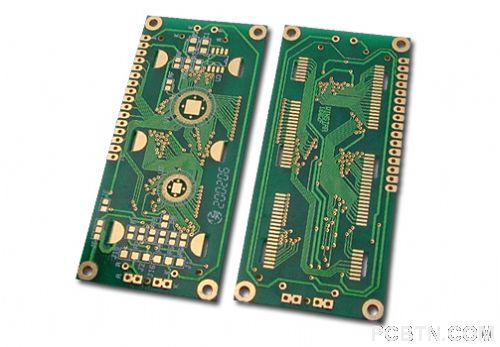
Section titled “What Is a PCB”A Printed Circuit Board (PCB), also called a printed wiring board, is defined at three levels:
- Printed circuit: a conductive pattern formed on an insulating base material according to a predetermined design — printed wiring, printed components, or a combination of both
- Printed wiring: the conductive pattern on an insulating base that provides electrical connections between components
- Printed circuit board (printed wiring board): the finished board carrying the printed circuit or printed wiring
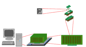
Electronic products are usually assembled in several levels — from the wafer (chip) at level 0, to the module at level 1, the card at level 2, the board at level 3, and up to the complete system. The PCB serves as the assembly base for level-1 components: it provides the mounting substrate on which modules and other electronic parts are assembled into a functional product.
Because the PCB connects every function of the product, when an electronic device fails, the PCB is often the first suspect. And since its fabrication process is relatively complex, production control must be especially strict.
A Brief History: From Hanson to Photoimage Transfer
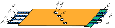
Section titled “A Brief History: From Hanson to Photoimage Transfer”- 1903 — Albert Hanson first applied the concept of “circuits” to telephone switching systems: conductors cut from metal foil were bonded between layers of paraffin paper — the prototype of today’s PCB construction.
- 1936 — Paul Eisner truly invented PCB fabrication technology and filed several patents. The core process of PCB manufacturing today — photoimage transfer — descends directly from his invention.
PCB Classification
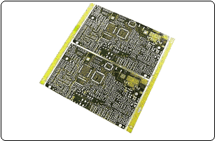
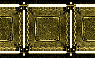
Section titled “PCB Classification”PCBs vary in material, layer count, and process to suit different products and requirements. Common classification dimensions:
| Dimension | Category | Notes |
|---|---|---|
| Material | Organic | Phenolic resin, fiberglass/epoxy (FR-4), polyimide, BT, etc. |
| Material | Inorganic | Aluminum, copper, and ceramic substrates — mainly for heat dissipation |
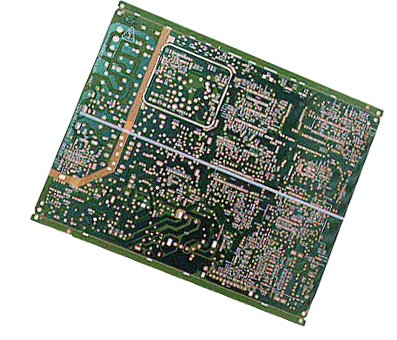
| Flexibility | Rigid PCB | Most common; FR-4 based |
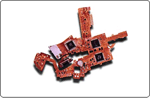
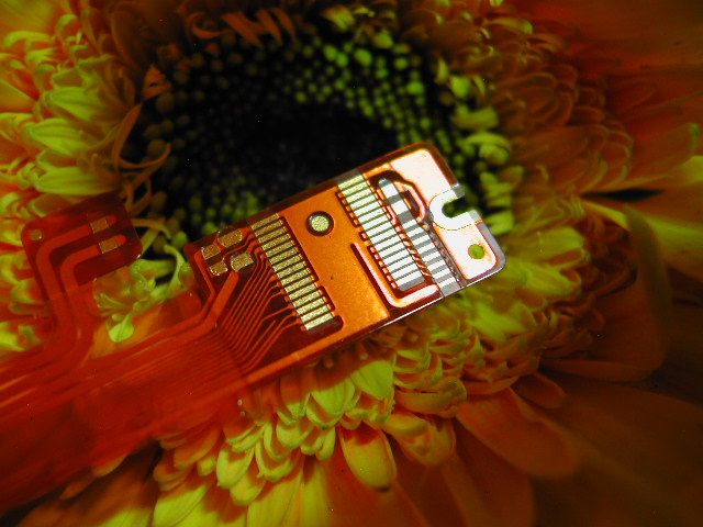
| Flexibility | Flexible PCB | Bendable; for space-constrained or dynamic applications |
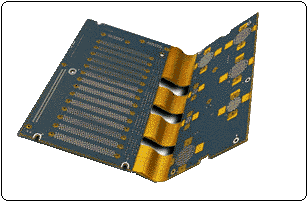
| Flexibility | Rigid-Flex PCB | Combines rigid and flexible regions |
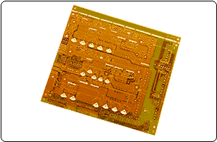
| Structure | Single-sided | Wiring on one side only; lowest cost products |
| Structure | Double-sided | Wiring on both sides, interconnected by vias |
| Structure | Multilayer | Multiple core boards laminated together for high-density interconnect |
The Eight Major Stages
Section titled “The Eight Major Stages”Using the multilayer board with the pattern plating process as the main thread, PCB manufacturing is divided into eight parts:
Eight stages of PCB manufacturing (multilayer, pattern plating)│├─ A. Inner Layer board cut → pretreat → lamination → exposure → developing → etching → strip → punching → inspection├─ B. Lamination & Drilling brown oxide → riveting → lay-up → pressing → post-treatment → drilling├─ C. Hole Metallization deburr → desmear → PTH → panel plating├─ D. Outer Layer Dry Film pretreat → lamination → exposure → developing├─ E. Outer Layer Circuit pattern plating → tin plating → strip → etching → tin stripping├─ F. Silkscreen solder mask printing → pre-bake → exposure/developing → legend printing → curing├─ G. Surface Finish finish selection (HASL / ENIG / OSP, etc.)└─ H. Final Processes profile → electrical test → final inspection → packing & shippingThe core of the inner layer stage is photoimage transfer + DES: DES stands for Develop, Etch, Strip — three processes run as one line. This is the key to understanding the entire PCB process, because the same “laminate → expose → develop → etch” logic reappears in later stages.

Series Navigation
Section titled “Series Navigation”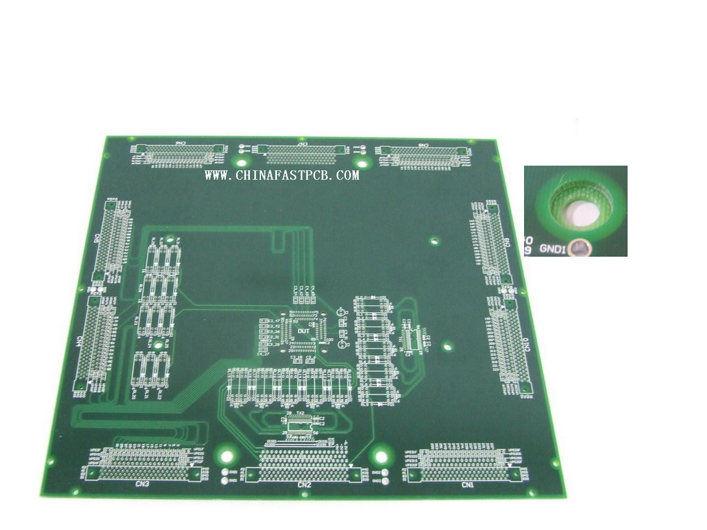
-
- PCB Manufacturing Overview (this article)
-
- Inner Layer Circuit Process: Photoimage Transfer and DES
-
- Lamination and Drilling
-
- Hole Metallization and Plating
-
- Outer Layer Circuit Process
-
- Solder Mask and Silkscreen
-
- Surface Finish and Final Processes
Summary
Section titled “Summary”- The PCB is the assembly base for module-level components; its manufacturing quality directly determines product reliability
- The core process idea is photoimage transfer (invented in 1936), classically implemented as DES and repeated throughout the flow
- The eight stages are closely linked — the following articles break down each one
We provide ESP32 ODM design-to-manufacturing services. From prototype to production — the team behind this tutorial can build it with you.
Talk to us →