Hole Metallization and Plating
Hole Metallization and Plating
Overview
Section titled “Overview”After drilling, the hole walls are insulating resin and glass fiber — the drilled holes still do not conduct. The purpose of hole metallization is to make the non-conductive parts of the hole wall (resin and glass fiber) metallic, providing a sufficiently conductive and protective metal wall for subsequent plating, and ultimately achieving electrical interconnection between all layers.
Process Chain Overview
Section titled “Process Chain Overview”Hole metallization process chain (C stage)Deburr → Desmear → PTH (Chemical Copper) → Panel Plating │ │ │ └─ plate to 200–500 μ" │ │ └─ chemically deposit a 20–40 μ" seed layer │ └─ remove hole-wall smear, expose copper rings └─ remove hole-entry burrs01 Deburr
Section titled “01 Deburr”- Cause of burrs: after drilling, uncut copper whiskers and uncut glass cloth remain at the hole edges
- Purpose: remove burrs at hole edges to prevent plating defects
- Main material: abrasive brushes
Burrs form tiny overhangs at the hole entry that hinder plating solution access and plating continuity — they must be removed first.
02 Desmear
Section titled “02 Desmear”- Cause of smear: the high temperature during drilling exceeds the resin’s glass transition temperature (Tg), turning the resin molten; as it cools, smear remains on the hole wall
- Purpose:
- Expose the copper rings of each layer that need interconnection
- Swelling agents improve the hole-wall structure and enhance copper plating adhesion
- Main material: KMnO₄ (potassium permanganate, the desmear agent)
Desmear is the critical prerequisite for hole metallization: smear covering the inner-layer copper rings causes “no copper in hole” or poor connection — one of the most common reliability failures in PCBs.
03 PTH (Chemical Copper)
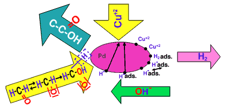
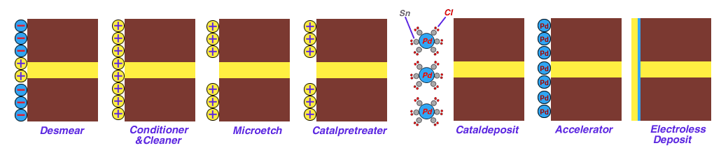
Section titled “03 PTH (Chemical Copper)”Purpose of PTH (Plated Through Hole): chemically deposit a layer of copper 20–40 micro-inches (about 0.5–1 μm) thick on the hole wall surface.
This ultra-thin copper layer is the “seed layer” for the whole metallization route — it turns the insulating hole wall into a conductive surface on which electroplating can build. The uniformity and adhesion of the chemical copper directly determine the long-term reliability of the via.
04 Panel Plating (First Copper)
Section titled “04 Panel Plating (First Copper)”- Purpose: plate 200–500 micro-inches (about 5–13 μm) of copper to protect the mere 20–40 micro-inch chemical copper from being damaged by later processes, which would cause barrel cracks (hole wall breaks)
- Main material: copper balls (anodes)
Panel plating plates the entire panel (including hole walls) uniformly. At this point the hole walls have a reliable conductive copper layer, and layer-to-layer electrical interconnection is physically established.
Summary
Section titled “Summary”- Four steps of hole metallization: Deburr → Desmear → PTH → Panel Plating, each depending on the last
- Key magnitudes: chemical copper 20–40 μ” (seed layer), panel plating 200–500 μ” (protective layer)
- “Smear” and “burrs” are the two enemies of hole metallization; barrel cracks and discontinuous plating usually trace back to them
- The board is now capable of interlayer conduction — next comes the outer layer: forming the final circuit pattern on the outer copper
Next up: the outer layer circuit process — using pattern plating (the positive process) to form the finished traces.
We provide ESP32 ODM design-to-manufacturing services. From prototype to production — the team behind this tutorial can build it with you.
Talk to us →