Solder Mask and Silkscreen
Solder Mask and Silkscreen
Overview
Section titled “Overview”Once the traces are formed, bare copper would oxidize in air and cause shorts during soldering. The silkscreen process (F stage) gives the PCB two “skins”: the solder mask (the protective layer over the outer traces, ensuring insulation, board protection, and solder resistance) and the legend (identification characters for maintenance and recognition).
Process Chain Overview
Section titled “Process Chain Overview”Silkscreen process chain (F stage)Pumice scrubbing → Solder Mask (print → pre-bake → expose → develop) → Legend (print → cure) │ └─ each side printed and pre-baked once: print side 1 → pre-bake → print side 2 → pre-bake01 Solder Mask
Section titled “01 Solder Mask”Solder mask is colloquially called “green oil”. To make visual inspection easier, the base lacquer usually contains green pigment that is easy on the eyes — though yellow, white, black, and other colors are also available.
Three purposes of solder mask:
- Solder resistance: keep the through-holes and pads to be soldered exposed, cover all traces and copper, prevent shorts during wave soldering, and save solder consumption
- Board protection: prevent moisture and electrolytes from attacking and oxidizing the traces (which would harm electrical performance), and prevent external mechanical damage, maintaining good surface insulation
- Insulation: boards are getting thinner and trace widths/spacings finer, making insulation between conductors increasingly critical — solder mask’s insulating performance matters more than ever
02 Solder Mask Pretreatment
Section titled “02 Solder Mask Pretreatment”- Purpose: remove surface oxides and increase surface roughness to strengthen ink adhesion
- Main material: pumice
03 Solder Mask Printing
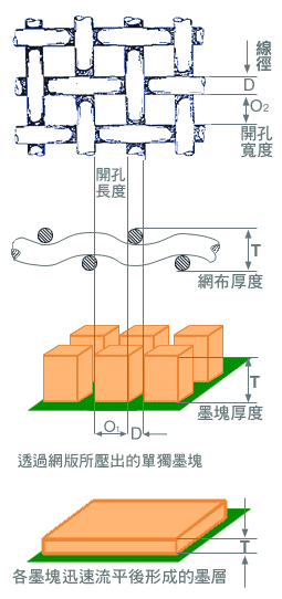
Section titled “03 Solder Mask Printing”Purpose: print the ink onto the board via a screen. Main material: ink.
Four common printing methods:
| Method | English |
|---|---|
| Screen printing | Screen Printing |
| Curtain coating | Curtain Coating |
| Spray coating | Spray Coating |
| Roller coating | Roller Coating |
04 Pre-bake
Section titled “04 Pre-bake”- Purpose: drive off solvents in the ink and partially harden it, so it does not stick to the photomask during exposure
- Process notes:
- Temperature and time must follow the supplier’s conditions; double-sided and single-sided printing need different pre-bake profiles
- The oven needs proper ventilation and filtration to prevent foreign matter from adhering
- Temperature and time must have alarms; boards must be removed the moment time is up — otherwise over curing causes incomplete developing
05 Solder Mask Exposure
Section titled “05 Solder Mask Exposure”- Purpose: image transfer
- Main equipment: exposure machine
- Process notes: machine cleanliness, energy selection, vacuum control
06 Solder Mask Developing
Section titled “06 Solder Mask Developing”- Purpose: remove the un-polymerized photosensitive ink with a 1% potassium carbonate (K₂CO₃) solution
- Main material: potassium carbonate
After developing, the pad areas are exposed (ready for soldering) while the rest of the copper is covered by solder mask.

07 Legend Printing
Section titled “07 Legend Printing”- Purpose: aid maintenance and identification (reference designators, polarity marks, board names, certification marks, etc.)
- Principle: screen printing (print one side, bake, then print the other)
- Main material: legend ink
08 Curing (Post-bake)
Section titled “08 Curing (Post-bake)”- Purpose: high-temperature baking to fully harden the epoxy resin in the ink
At this point, the “protective layer + identification layer” of the board surface is complete.
Summary
Section titled “Summary”- Three purposes of solder mask: solder resistance (prevent shorts in soldering), board protection (against oxidation and damage), insulation (isolate conductors)
- The solder mask process = pretreat → print → pre-bake → exposure → developing → curing — photoimage transfer in a photosensitive ink version
- Pre-bake is the critical control point: too little sticks to the film, too much (over curing) causes incomplete developing
- The legend layer is applied by screen printing and serves assembly and repair downstream
Next up, the finale: surface finish (protecting the exposed pad copper) and final processes (profiling, electrical test, final inspection, shipping).
We provide ESP32 ODM design-to-manufacturing services. From prototype to production — the team behind this tutorial can build it with you.
Talk to us →