Surface Finish and Final Processes
Esta página aún no está disponible en tu idioma.
Surface Finish and Final Processes
Overview
Section titled “Overview”Once the solder mask covers the traces, the copper at the pads remains exposed — unprotected, it would oxidize and undermine soldering. The surface finish (G stage) dresses this copper in an anti-oxidation “protective coat”, while the final processes (H stage) complete profiling, electrical testing, final quality inspection, and packing.
This article concludes the series, ending with a recap of the full 19-step route.
Surface Finish (G Stage)
Section titled “Surface Finish (G Stage)”Every conventional PCB has copper layers; unprotected copper oxidizes and degrades, directly affecting soldering. There are seven common protective finishes:
| Finish | Full name | Key point | Advantages |
|---|---|---|---|
| HASL | Hot Air Solder Leveling | The board is fully coated with solder, then high-pressure hot air blows off the excess on the surface and in the holes and levels the rest; leaded and lead-free versions | Low cost; stays solderable throughout the process |
| OSP | Organic Solderability Preservative | Forms a thin, uniform protective layer on the copper | Cost comparable to HASL; good coplanarity; lead-free process |
| Plating Gold | Electroplated Nickel Gold | Electroplates nickel and a protective gold layer onto copper | Good solderability; flat surface; long shelf life; withstands multiple reflows |
| ENIG | Electroless Nickel Immersion Gold | Chemical displacement deposits a nickel-phosphorus layer, then a gold layer on top | Good solderability; flat surface; long shelf life; withstands multiple reflows |
| Gold Finger | — | Electroplated nickel-gold with a different gold composition (hard gold, wear-resistant) | Wear-resistant, low contact resistance; used for edge connectors |
| Immersion Silver (IS) | — | Immerses a 0.1–0.6 μm silver layer onto the copper | Good solderability; flat surface; a natural HASL replacement |
| Immersion Tin (IT) | — | Immerses a 0.8–1.2 μm tin layer onto the copper | Good solderability; flat surface; relatively low cost |
Selection usually depends on: soldering process (lead-free/leaded), shelf life, cost, and appearance requirements (ENIG has become a common choice for high-end products).
Final Processes (H Stage)
Section titled “Final Processes (H Stage)”01 Profiling
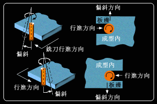
- Purpose: cut the board to the customer-specified dimensions
- Principle: mechanical cutting by CNC machines
- Main material: router bits
- Common forms: CNC routing, and V-cut (V-shaped scoring) — used for panel pre-scoring so finished boards snap apart along the groove; requires controlling the cut depth and remaining web thickness

02 Electrical Test
- Purpose: bare-board testing of PCB electrical performance (opens and shorts) to meet customer requirements
- Trade-offs among test methods:
| Method | Principle | Pros | Cons | Best for |
|---|---|---|---|---|
| Dedicated | Custom bed-of-nails fixture | Fast throughput | Probes cannot be reused; high fixture cost | High volume |
| Universal on Grid | Universal grid fixture | Lower fixture cost | High equipment cost | Medium-high volume |
| Moving Probe (flying probe) | Two probes move in X/Y/Z to test each net’s endpoints in turn | No fixture; low cost | Low throughput | Samples, small batches, rush samples |
03 Final Inspection and Laboratory
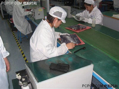
Final inspection/lab is the last quality review in the process, in two categories:
- Inspection items (appearance and dimensions): outline dimension, hole-to-edge distance, board thickness, hole diameter, line width/space, annular ring, and more
- Laboratory items (reliability): solderability, peel strength, micro section, thermal shock, ionic contamination, moisture and insulation resistance, impedance, and more
04 Packing and Shipping
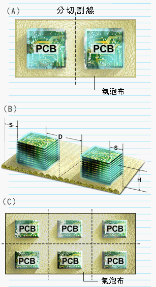
The board is packed as the customer requires and shipped — completing the full journey of a PCB.
The Full 19-Step Recap
Section titled “The Full 19-Step Recap”Expanding the eight stages into one line gives the complete PCB manufacturing route:
1. Inner layer 2. Lamination 3. Exposure 4. Developing 5. Etching6. Strip 7. Lay-up 8. Pressing 9. Drilling 10. PTH11. Lamination 12. Exposure 13. Developing 14. Cu+Sn plate 15. Strip16. Etching 17. Tin strip 18. Silkscreen 19. Surface finish → final processes → shippingNotice: the photoimage transfer and DES logic — “laminate → expose → develop → etch → strip” — appears three times (inner layer, outer layer, solder mask, in different forms). That is the process main thread emphasized in the first article.
Summary (Series Wrap-up)
Section titled “Summary (Series Wrap-up)”- The seven surface finishes each have trade-offs; the ENIG/OSP/HASL choice directly affects solderability and cost
- The final processes handle three things: cut the profile (routing + V-cut), test opens/shorts (three test methods), and inspect before shipping (appearance + reliability checklists)
- Full recap: board cut → inner layer → lamination → drilling → metallization → outer layer → silkscreen → surface finish → final processes — 19 steps across eight stages
You have now walked the complete professional PCB manufacturing process. Recommended next reads:
- Chapter 24 (PCBA Manufacturing and Soldering) — assembling the bare board into a PCBA
Every step from “design file to manufactured part” deserves to be seen with your own eyes (or in a video). Understand the process, and you will make better designs.
We provide ESP32 ODM design-to-manufacturing services. From prototype to production — the team behind this tutorial can build it with you.
Talk to us →