Inner Layer Circuit Process: Photoimage Transfer and DES
Esta página aún no está disponible en tu idioma.
Inner Layer Circuit Process: Photoimage Transfer and DES
Overview
Section titled “Overview”Multilayer board fabrication starts with the inner layer circuit: using photoimage transfer to create the first circuit pattern on copper-clad laminate. The sequence “lamination → exposure → developing → etching → strip” is the template for the entire PCB process — outer layers and solder mask follow the same logic in later stages. Master this article and the rest of the flow becomes easy to follow.
Process Chain Overview
Section titled “Process Chain Overview”Inner layer process chainBoard Cut → Pretreat → Lamination → Exposure → Developing ─┐ ├─ DES (Develop · Etch · Strip) Etching → Strip ──────────┘ → Punching → AOI InspectionDevelop, Etch, and Strip are often run as a single production line, abbreviated as DES.
01 Board Cut
Section titled “01 Board Cut”Purpose: cut the base material to the working size required by the pre-production engineering plan.
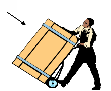
Main material: copper-clad laminate (copper foil laminated onto an insulating layer). Boards come in various thickness specifications; by copper thickness they are classified as H/H, 1oz/1oz, 2oz/2oz, and so on (1oz ≈ 35 μm of copper).
Notes:
- Avoid edge burrs affecting quality: grind and round the edges after cutting
- Account for material expansion/contraction: bake the cut panels before sending them to the next process
- Cutting must respect the warp/weft direction matching the engineering instructions to avoid warpage
02 Pretreat
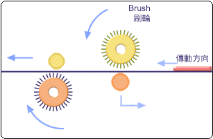
Section titled “02 Pretreat”Purpose: remove contaminants from the copper surface and increase surface roughness to prepare for the subsequent lamination step.
Main consumable: abrasive brushes.
After pretreatment, the copper surface becomes microscopically rough so the dry film can bond firmly — insufficient roughness leads to side etching and film peeling during later etching.
03 Lamination (Dry Film)
Section titled “03 Lamination (Dry Film)”Purpose: hot-press a dry film resist onto the treated copper surface.
Main material: dry film (a photosensitive resist material that acts as the protective layer for etching).
04 Exposure
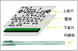
Section titled “04 Exposure”Purpose: transfer the image on the original film onto the photosensitive board by light irradiation.
Main tool: film / photomask.
Principle: UV light passes through the film to expose the dry film — the transparent (white) areas undergo photopolymerization, while the opaque (black) areas do not react. During developing, the polymerized areas cannot be dissolved and remain on the board.
At this point, “which copper will survive” has been decided by the film: transparent areas correspond to the traces that will remain.
05 Developing
Section titled “05 Developing”Purpose: use an alkaline solution to wash away the dry film that did not react.
Main material: K₂CO₃ (potassium carbonate) solution.
Principle: water-soluble dry film contains organic acid groups that react with weak alkali to form organic acid salts, which dissolve in water — so the unexposed (unpolymerized) dry film is washed away, exposing the copper beneath, while the polymerized dry film stays as the etch resist.
06 Etching
Section titled “06 Etching”Purpose: use chemical solution to etch away the copper exposed after developing, forming the inner layer circuit pattern.
Main material: etching solution (CuCl₂, copper chloride).
The bare copper regions are etched away while film-protected copper remains — the dry film pattern literally becomes copper traces.
07 Strip
Section titled “07 Strip”Purpose: use strong alkali to strip the resist layer protecting the copper and reveal the circuit pattern.
Main material: NaOH (sodium hydroxide).
After stripping, the inner layer pattern is fully revealed — completing the DES trio and producing a core board with only its inner layer pattern.
08 Punching
Section titled “08 Punching”Purpose: use CCD registration to punch the locating holes for inspection and the rivet holes for subsequent lamination.
Main material: drill bit. Locating holes are the datum for all subsequent registration processes — their accuracy directly affects layer-to-layer alignment.
09 AOI Inspection
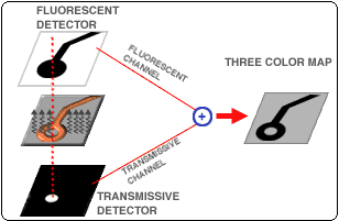
Section titled “09 AOI Inspection”AOI (Automatic Optical Inspection):
- Purpose: feed an optically reflected image back to the equipment, compare it against set logic criteria or the reference pattern, and locate defects
- Common defect types:
- Open / Fine Open
- Short / Fine Short / Surface Short
- Nick / Protrusion
- Pinhole / Copper Splash
- Missing Pad / Overetched
- Note: because AOI works by logic comparison, some false calls are inevitable and must be confirmed by human review — AOI filters, humans adjudicate
Summary
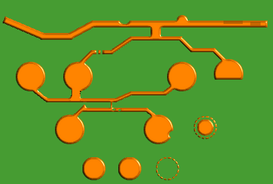
Section titled “Summary”- The inner layer = photoimage transfer + DES, the standard demonstration that every later circuit process is a variant of
- Exposure decides the pattern (the film), developing reveals it, etching shapes it, stripping exposes it
- Warp/weft direction, lamination shrinkage, and punching accuracy are quality seeds planted at this stage
- AOI is the first quality gate, but it needs human adjudication
Next up: lamination and drilling — pressing inner cores and outer foils into a multilayer board, and drilling the vias that connect the layers.
We provide ESP32 ODM design-to-manufacturing services. From prototype to production — the team behind this tutorial can build it with you.
Talk to us →